Today, AMD’s Radeon Technologies Group is finally revealing their 4th generation GCN GPU architecture, aka Polaris.
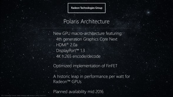
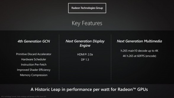
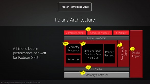
AMD’s Polaris architecture will include a number of new improvements to the previous generation GCN architecture including a primitive discard accelerator, hardware scheduler, instruction pre-fetch, improved shader efficiency and improved memory compression algorithm. Along with that is also support for HDMI 2.0a as well as DisplayPort 1.3. 4K/60FPS H.265 hardware encode/decode will also be built into the chip.
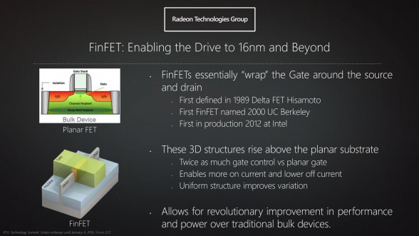
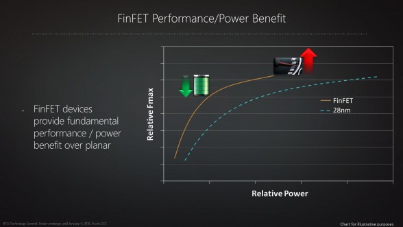
The biggest improvement to the Polaris architecture however is power efficiency, which is achieved through a combination of a new manufacturing node and architectural improvements. Whereas current generation AMD chips are produced on the 28nm process, Polaris GPUs will be manufactured on a combination of 16nm FinFET (TSMC) and 14nm FinFET (Global Foundries/Samsung) manufacturing processes.
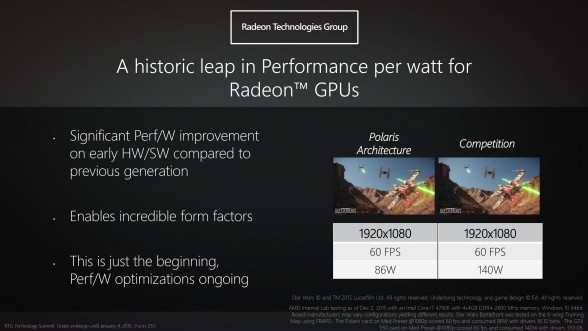
AMD claims that their efficiency improvements will result in up to 61% reduction in power consumption against competing GPUs. Comparing a yet unannounced GPU based on the new Polaris architecture against the Nvidia GeForce GTX 950 (Maxwell) in Star Wars Battlefront at 1080p/60FPS medium settings, the Polaris based GPU required just 86w against the GTX 950’s 140w.
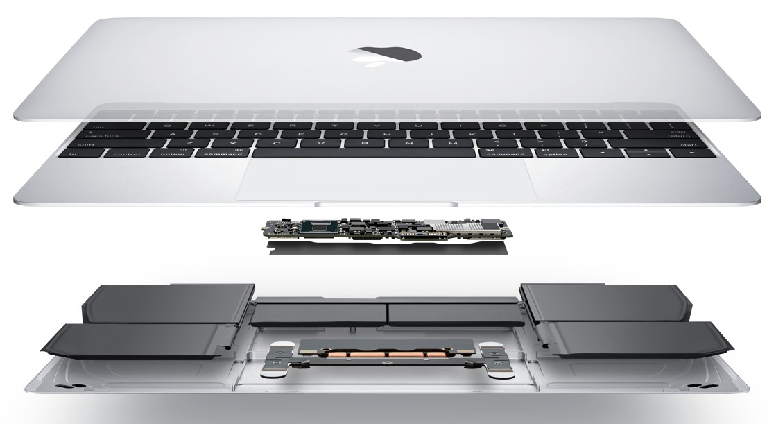
Overall, this is some pretty exciting news as AMD graphics technology hasn’t seen much energy efficiency improvements in the past few years. Thanks to better efficiency, we should also be seeing significantly more powerful graphics in notebook applications as well. AMD expects to launch Polaris based GPUs in mid-2016 which is still about 6 months away, so we’ll likely see more information about it trickle in the next few months. Nvidia is expected to launch their next generation Pascal GPUs based on 14nm FinFET during this timeframe as well, so 2016 should be a pretty exciting year for GPU technology. Stay tuned!

