At Intel’s recent Technology and Manufacturing Day, Intel presented more details regarding its 10nm FinFET manufacturing process. In the presentation materials, Intel highlighted some of the major improvements that its 10nm FinFET process will bring.
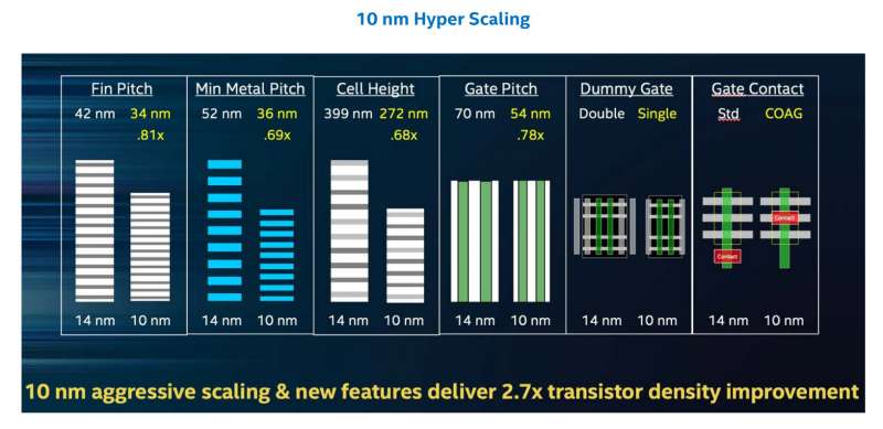
In order to cram even more transistors than ever before, Intel is using both traditional scaling techniques along with a few new ones which they call Hyper Scaling.
Pitch, or the distance between its components, has been improved significantly thanks to Intel’s new Self-Aligned Quad Patterning technique. As a result, Intel’s 10nm transistor reduces the minimum fin pitch from 42nm to 34nm, minimum gate pitch from 70nm to 54nm, and the minimum metal pitch from 52nm to 36nm. This allows more transistors to be packed closer together in a certain area.
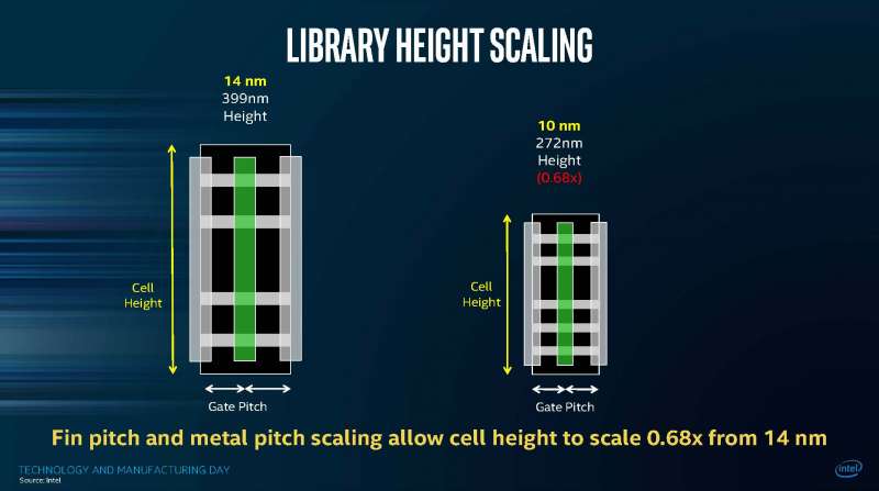
Improved transistor size also reduces the cell height – that is, a group of transistors connected together to form a binary logic. Intel’s 10nm transistor has a minimum cell height of 272nm compared to 14nm’s minimum cell height of 299nm.
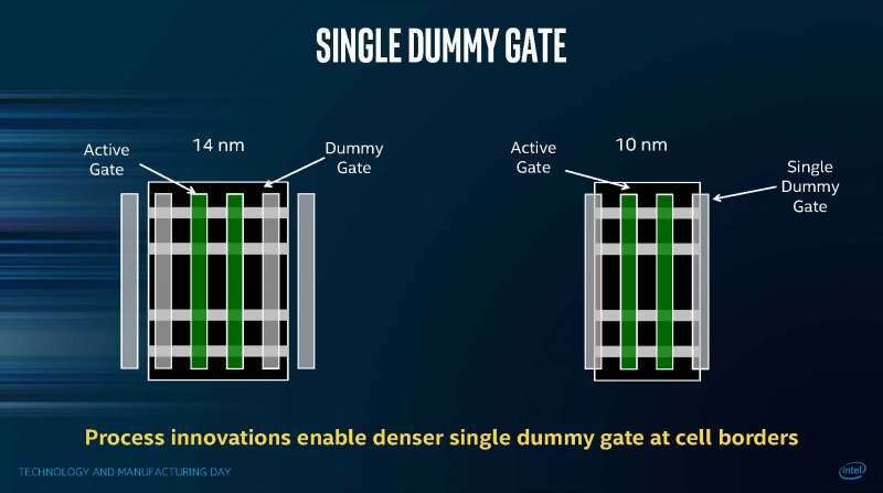
Intel also introduced two new methods of improving transistor density, which it refers to collectively as Hyper Scaling. Hyper Scaling includes Single Dummy Gate and Contact Over Active Gate (COAG).
Dummy gates are the insulation that separates the each cell from one another. With Intel’s 10nm FinFET, each logic cell only requires one dummy gate to act as insulation, significantly improving density.
To enable/disable a transistor, a voltage needs to be applied to the gate part of a transistor via a metal contact. Traditionally, the gate contact is placed on the side of the transistor. With Intel’s 10nm transistor, the gate contact is now stacked with the transistor itself to save even more space.
As a result of Intel’s aggressive pitch scaling along with Hyper Scaling made possible by their advanced Self-Aligned Quad Patterning techniques, up to 100.8 million 10nm FinFET transistors can be squeezed into 1mm² area resulting in a 2.7x density increase over its 14nm FinFET process despite a less than 30% reduction in feature size.
Combined with significantly decreased SRAM area, die area of 10nm continues to shrink at a 0.43x over previous generation 14nm.
The cost of transistors also continues to decrease at the same rate as previously expected.
With more transistors packed into the same space, this allows Intel’s 10nm FinFET process to deliver up to 25% better performance and 45% lower power consumption than its 14nm FinFET process. Because of Hyper Scaling, Intel claims their 10nm will be a full generation ahead of competing 10nm processes.
After 10nm FinFET goes into mass production, Intel will release an enhanced version of the 10nm process called 10+ followed by 10++. Intel’s 10++ process is expected to boost performance by another 15% and reduce power consumption by an additional 30%. This is the same strategy we’ve seen on Intel’s 14nm process.
Intel expects its 10nm based chips to begin manufacturing in 2H2017 and begin shipping by the end of this year.
Source: Intel


