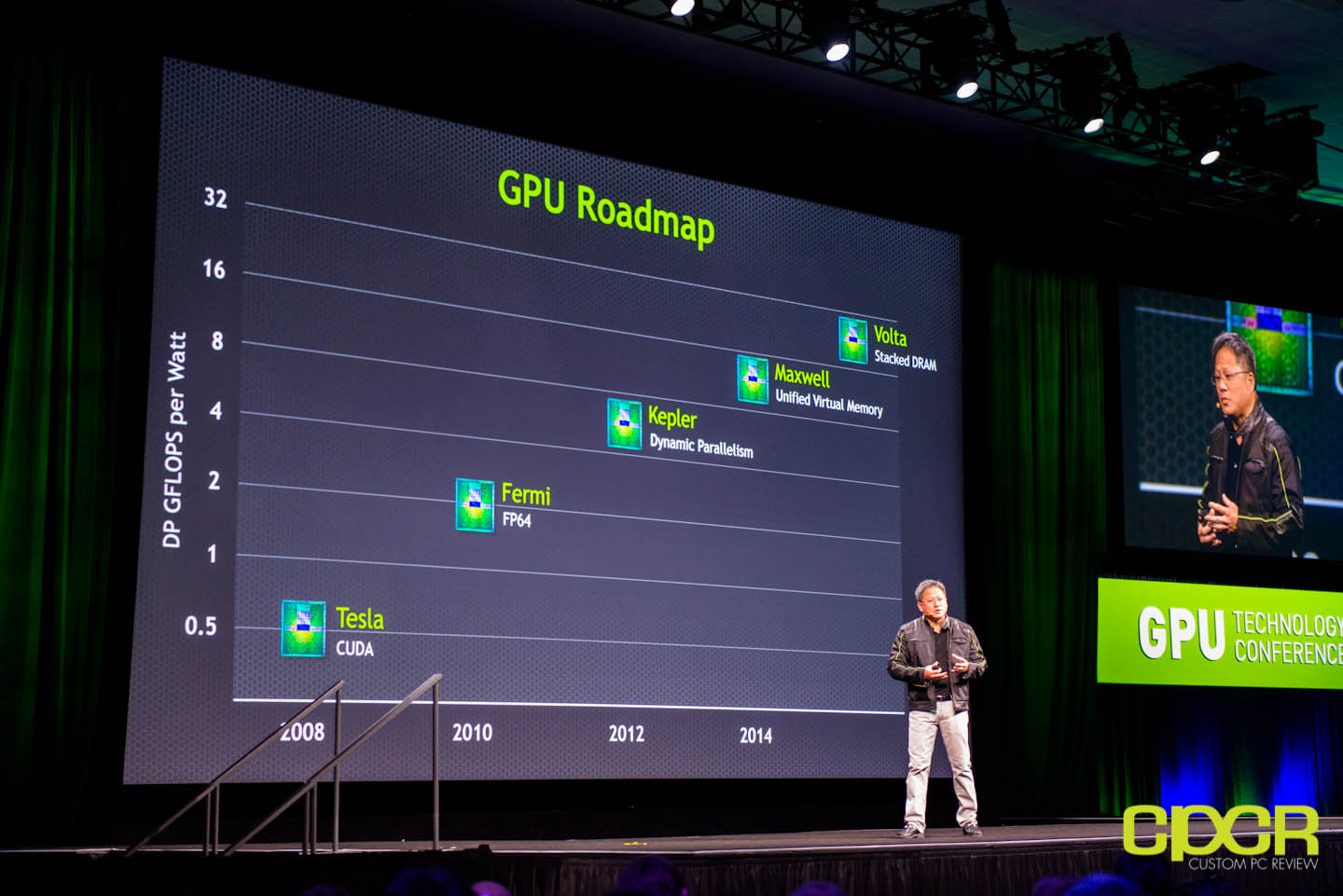
Recently at Nvidia’s GTC (GPU Technology Conference) 2013 conference, Nvidia CEO Jen-Hsun Huang talked briefly about Nvidia’s GPU roadmap containing next generation Maxwell and Volta GPU architectures.
Whereas current generation Kepler’s major feature is dynamic parallelism, Maxwell furthers this with a unified virtual memory. This allows the memory in the GPU to be accessed directly by the CPU, and memory in the CPU to be accessed via the GPU, which in turn helps increase power efficiency, performance and promote better programmability. Maxwell, which was first introduced to us in late 2010 appears to be coming sometime in 2014 and will be succeeding current generation Kepler architecture.
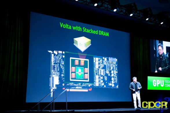
Following the Maxwell architecture will be the Volta architecture, which is largely focused on improving power efficiency while simultaneously improving graphics performance. Jen-Hsun indicated that one of the largest limitations to GPUs today is access to memory bandwidth, so with the Volta architecture Nvidia is integrating the DRAM directly onto the die. Since memory ICs are traditionally individually surface mounted on a PCB, in order to do this Nvidia is utilizing stacked DRAM technology, which as its name implies stacks DRAM memory on top of each other. By integrating the memory onto the GPU die, the Volta GPU is expected to gain access to up to 1 TB/s memory bandwidth. In comparison, the Nvidia Titan (Nvidia’s current most powerful single GPU graphics card today) only provides a maximum of up to 288.4 GB/s memory bandwidth. No expected release date has been confirmed, but with Fermi’s launch in 2010, Kepler’s launch in 2012, and Maxwell’s launched expected in 2014, it’s probably a safe bet that we’ll be seeing Volta sometime in 2016.

