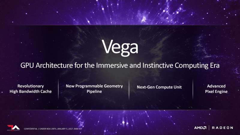
Alongside Ryzen, the Vega GPU is considered by many as AMD’s spearhead product for 2017. As it’s is slowly being finalized for mass production, we had the pleasure of meeting up with Scott Wasson and discuss the details of what Vega can bring to the table.
Scott started off the meeting by pointing out a major problem floating in the graphics industry today: graphics memory could no longer keep up with the demand of the processing power. In addition, conventional GPU architectures can’t adequately scale to handle big data. The media creation industry is using petabytes of working data, and the deep learning sector is extending into the exabytes range.
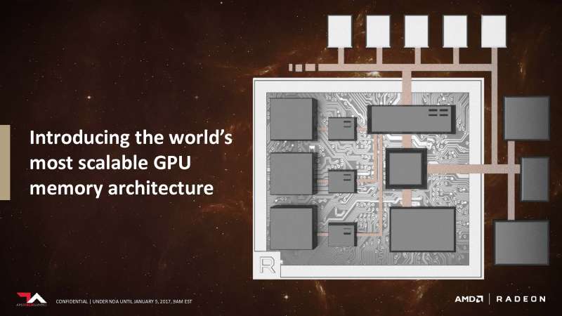
AMD claims that the Vega architecture will feature the most advanced memory management to date from AMD.
One of AMD’s highest priorities is to optimize memory performance to tailor to the variety of workloads as well as the sheer quantity. One of many measures, but by far the most critical, is to use high-bandwidth memory.
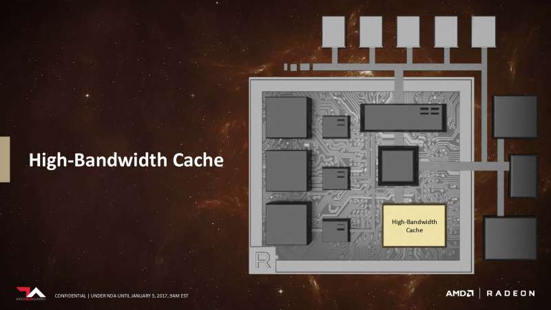
As graphics technology continue to evolve, the term “frame buffer” no longer applies in the conventional sense. Graphics memory has been designed to handle a variety of tasks for some time now, which is why AMD has decided to name its upcoming generation of graphics memory “High-Bandwidth Cache”. High-bandwidth memory was first seen on the Fury X graphics cards. Instead of using planar GDDR5 memory, AMD installed vertically stacked memory onto an interposer with the GPU, reducing trace travel distance while massively increasing bandwidth. Due to limitations of the first generation of HBM, the maximum memory capacity for each stack was limited to 1GB. Not only that, only 4 stacks could be installed on the interposer around the GPU die.
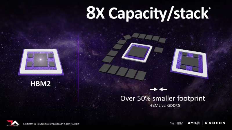
With Vega, everything is about to change. HBM2 increases the memory stack height to 8. According to AMD, HBM2 offers 2x bandwidth per pin vs HBM1. Considering how HBM2 has twice the capacity as HB1, this increase in bandwidth is needed to use the memory at peak performance.
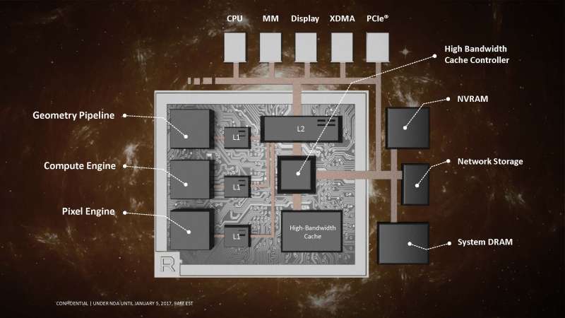
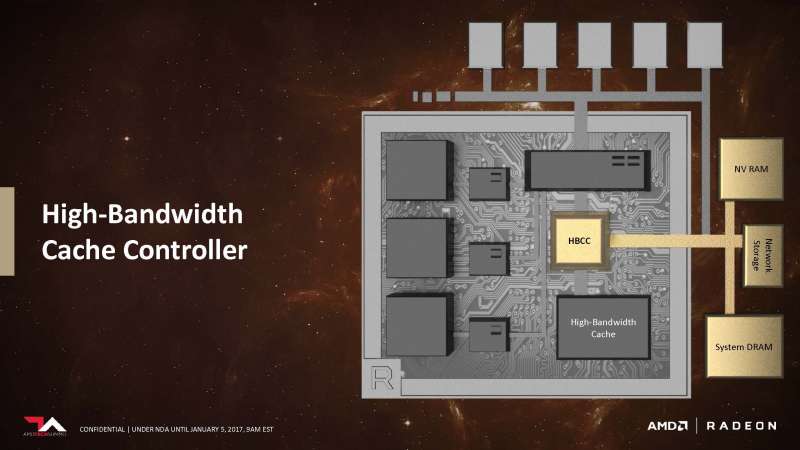
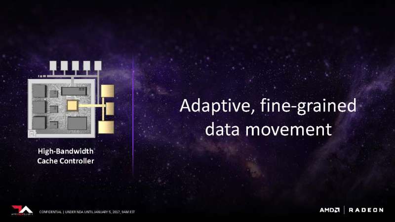
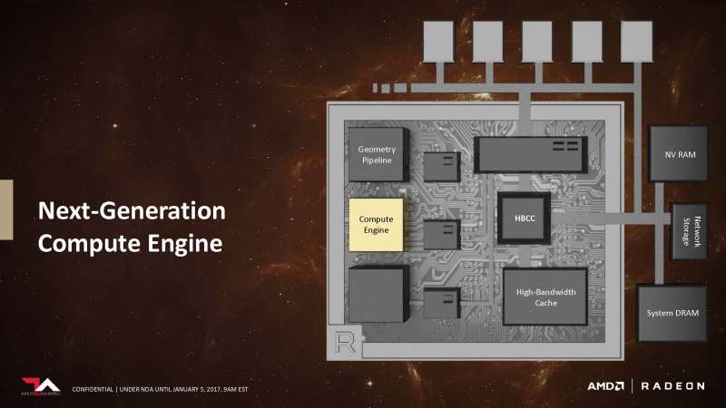
While having a robust high-bandwidth cache on-chip is important, Vega’s High-Bandwidth Cache controller extends beyond that. HBCC can also address external storage types as cache. Components such as system DRAM, NV (non-volatile) RAM and even network storage devices can be used to cache data needed for the GPU. You don’t actually have to wait until Vega is released to see this feature in action, remember how the recently released Radeon SSG workstation card carried a 1TB SSD on-card but are separate from the graphics system? That’s what it’s used for.
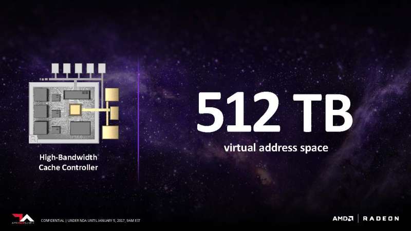
With that in mind, it’s no surprise that AMD boasts that Vega can theoretically address 512TB of virtual address space. The HBCC will also be able to mix and match which cache type is best suited for the workload on hand.
A prominent feature for gaming optimization is adaptive, fine-grained data movement. Essentially, what this does is allow for granular control of the assets being stored in the GPU’s VRAM.
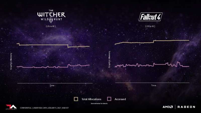
To demonstrate a usage scenario for adaptive fine grain movement, AMD showed us a graph of how most of today’s games allocate graphics memory. Most games only access and render out about half of the graphics memory they reserve, leaving a huge chunk of unused overhead. AMD hopes to alleviate this situation by dynamically allocating the memory based on the access pattern and reserve memory more closely to the demand of the operation. This is possible thanks to Vega’s High Bandwidth Cache and new HBC controller, which allows developers to swap data in and out of the framebuffer more quickly and without the added latency and performance reduction you’d see on previous architectures. AMD claims these enhancements will effectively double the GPU’s memory capacity, which is a rather bold statement.
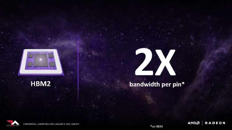
HBM2’s memory interface is double that of HBM1. Each pin can transmit 2x the bandwidth. What this means is that while the Vega GPU die AMD showed off appears to have only two stacks of HBM2 memory compared to the four stacks of HBM1 found on the Fiji GPU (Fury X), it can still theoretically offer the same memory bandwidth while offering a higher capacity and smaller footprint compared to HBM1.
Of course, compared to traditional planar GDDR5 which requires the memory to be spread across a large area, HBM2 offers a significantly smaller footprint. This leaves more room for other components and features, or reduce the length and cost of the PCB altogether.
AMD showcased a scene from Deus X: Mankind Divided. When the textures are stripped, the wireframes show that there are nearly 20 million polygons in a single frame. Scott explains that some of these objects can be as small as a pixel. In the enterprise simulation sector, the workload is even heavier. A typical workload can reach north of 200 million geometries per frame.
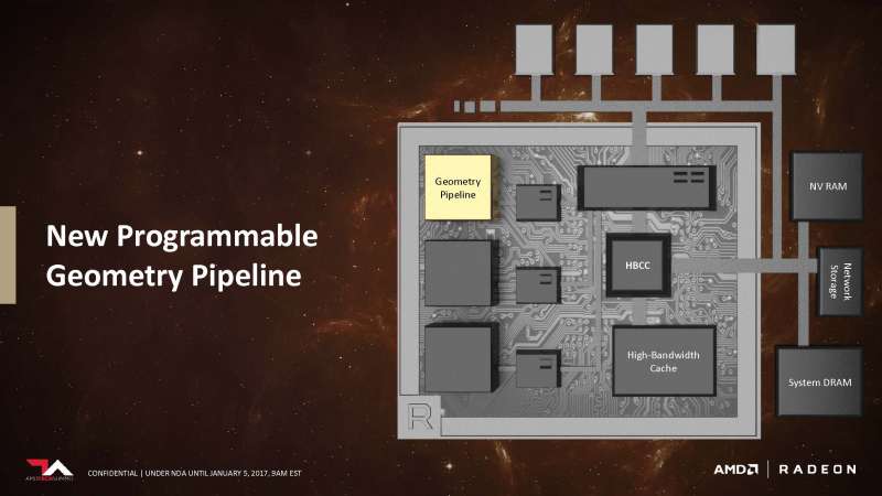
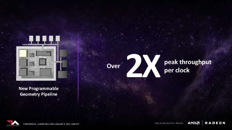
To tackle all these problems, AMD has redesigned the geometry engine and changed the pipeline geometries are rendered. Steps such as culling and primitive discard have all been improved over the existing design. On top of which, the geometry pipeline is now programmable.
Overall, the efficiency of the architecture was able to improve the peak throughput per clock compared to the original design. It looks like this time around, AMD is actually improving the efficiency of the shaders. AMD didn’t go into much detail about how they achieved this technically, but keep in mind that this is report is just a tidbit of what’s to come.
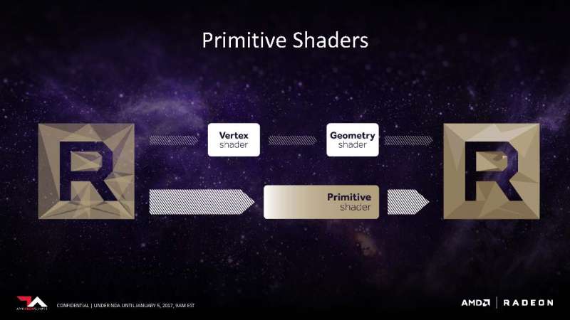
Vega will allow geometry and vertex shaders to be programmed via Primitive Shaders. In the traditional sense, the shading process is a fixed pipeline that follows a script of steps. With Primitive Shaders, the vertex and geometry shaders are technically being considered as primitives. This is very helpful in a feature called primitive discarding, where objects that are blocked from view get discard before outputted on screen. By reducing vertex and geometry shader into primitives allows for more efficient and faster hardware discarding, which can greatly reduce overhead on the GPU workload. AMD has stated that this technology needs to be exposed by an API or within the driver. Currently, DX12 does not support exposing primitive shaders, but that doesn’t mean it can’t be added in the future.
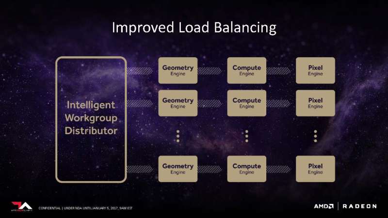
The intelligent Workgroup Distributor can now spread workloads on more than 4 Shader Engines. Each shader engine composes of a geometry engine, compute engine, and a pixel engine.
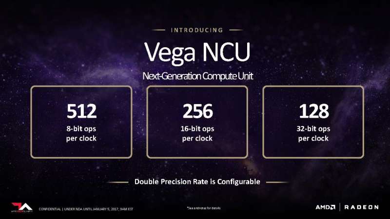
One of AMD’s goal with Vega is to make the NCU as flexible as possible. The slide above demonstrates how the number of operations per clock scales based on the length of the instructions: the shorter the instructions, the more operations can be processed per clock.
To understand why this is crucial, we have to understand where these data types are used. The slide above caters strictly to floating-point numbers, which is just a fancy term for a decimal number. Popular types of floating point numbers include 8-bit , 16-bit, 32-bit, and 32-bit. Each length is useful for a different workload. For example, in deep learning, 8-bit float is extremely popular because data volume is prioritized over precision (precision is generated using an average of volume). In gaming, 16-bit are required to describe lighting, physics, and other numerical values that require such level of precision. By making performance scale with the workload on hand, Vega can become a workhorse in both gaming rigs and data centers.
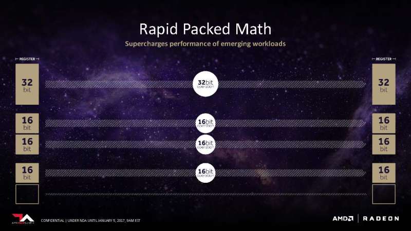
The secret to the scaling lies within the registers. The 32-bit FPU register in Vega can be split into multiple, lower bit FPU register if the instructions are similar in kind and width. Compared to the old architecture where the register must wait to be cleared no matter the length of the datatype, the new design in Vega can potentially double and quadruple the instructions per clock in certain scenarios. When it encounters a continuous stream of 16-bit operations, it can actually disable half the register to increase performance and decrease overhead. All the mumbo-jumbo translates to one thing: Higher instructions per clock (IPC).
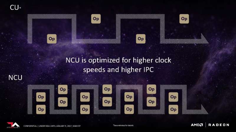
So how do you push more data when you have already perfected IPC? Boost the clock speed of course! Compared to the Compute Unite (CU) from the previous generation, the NCU in Vega could push more clock and reduce the latency between operations.
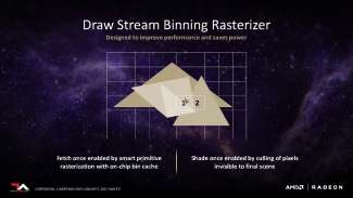
With Vega, AMD has fundamentally changed the way the way geometries are rasterized. Rasterization is the process of converting the rendered geometries into the pixels displayed on-screen. It’s also the stage where obstructed/unseen parts of the frame are clipped and culled. Historically, AMD has used immediate-mode rasterization that rasterized on the entire screen before moving onto the next stage. It’s a dated method but it worked well for its time.
AMD’s new Draw Stream Binning Rasterizers uses tile-based rasterization. Instead of drawing the screen all at once, tile-based rasterization divides the screen into smaller “blocks” and rasterizes the components inside each block individually. The blocks are then stitched together to form the final scene. Tile-based rasterization offers two distinct advantages. One: by working with a smaller block, the amount of memory required to store data is significantly reduced. This means that the vertices and their associated information can now be worked into the on-chip bin cache without having to load it into memory. Two: Because each block is rasterized from start to finish before moving on to the next, the rasterizer only needs to make one pass on the screen to perform all the necessary clipping and culling functions.
Nvidia has been using tile-based rasterization since Maxwell. According to AnandTech, it was an attributing factor to its performance leap from Kepler. It’s also a technique traditionally used in mobile SoCs such as Qualcomm’s Adreno. The goal of DSBR is to save power and improve performance in various instances it can increase effective memory bandwidth on lower-end parts, but also reduce power consumption on higher-end graphics solutions as well.
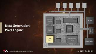
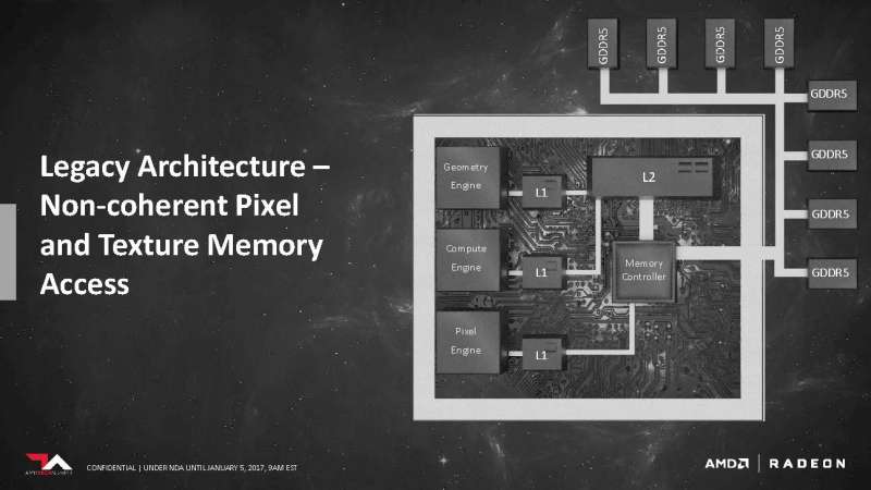
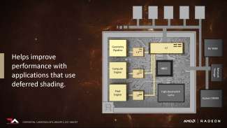
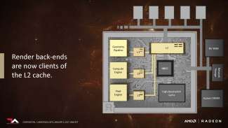
With the new architecture, the Pixel engine no longer has to go through the memory controller before it can access the L2 Cache. In addition, the L2 Cache doesn’t need to be cleared before being accessed nor will it interfere with operations performed on the cache by other components. We think this is also where the rasterized frame is being kept on-chip, so by allowing the pixel engine to access the L2 cache directly could potentially enable some of the pre-rasterized assets to be reused for the next frame.
To sum it up, there are four pillars for Vega’s success: High-Bandwidth Cache (HBM2), Programmable Geometry Pipeline, NCU, and a new Pixel Engine. Vega is expected to release in the first half of 2017. AMD was not ready to detail any specific products, but they did point out that the first product which was demoed running DOOM at 4K at over 60 FPS, was aimed at the high-end market segment. When asked about whether all Vega cards will be carrying HBM2, AMD gave us the good ol’ shrug and smile. AMD also said the press deck only reveals a portion of Vega’s features, so stay tuned for more juicy info as they appear.
Tom Li contibuted to this report.

