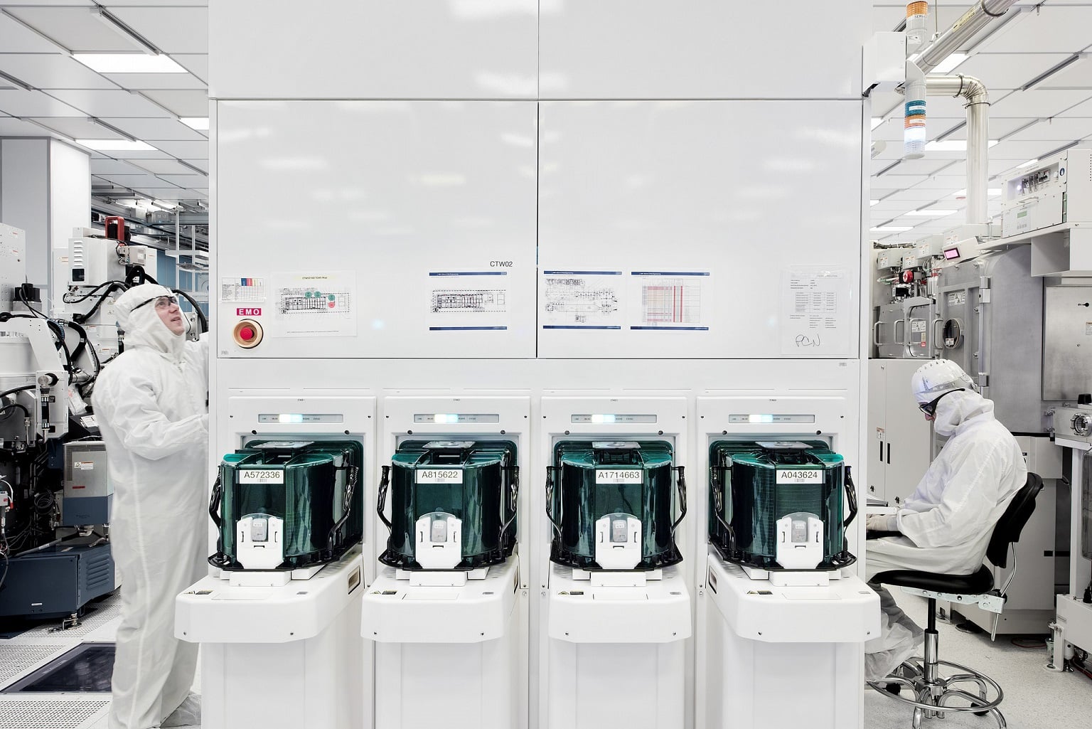
IBM Research Alliance recently announced that they’ve developed a process to produce the world’s first 5nm transistors. The new transistors will allow IBM to squeeze as much as 30 billion transistors into a chip just 50mm² resulting in as much as 40% improvement in performance at the same power or a 75% reduction in power at the same level of performance when compared to current generation cutting edge 10nm technology.
In order to shrink the transistors down to the 5nm feature size, IBM researchers spent 10 years developing a new technology which they call Stacked Nanosheet Gate-All-Around Transistor (GAAFET) technology.This simpler design was then combined with EUV (Extreme Ultraviolet) manufacturing technology to produce the new chips.
No word on when IBM or its development partners (Samsung, GlobalFoundries) will begin commercializing 5nm chip technology however, GlobalFoundries has previously announced that they expect to roll out 7nm chip technology in 2018. More information about the new technology will also be provided at the 2017 Symposia on VLSI Technology and Circuits conference in Kyoto, Japan.
Source: IBM


