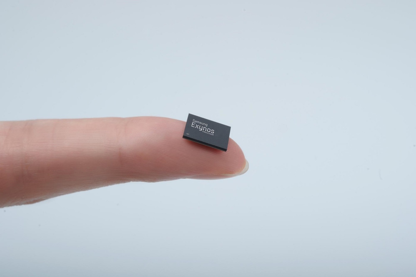
According to a recent announcement, Samsung has begun mass production of the industry’s first 10nm FinFET SoCs further solidifying Samsung’s position as one of the world’s most advanced chipmakers.
Samsung’s 10nm FinFET process will include two products – the Samsung 10nm FinFET LPE and the Samsung 10nm FinFET LPP. The Samsung 10nm FinFET LPE process, which is currently being mass produced, is designed with power efficiency in mind for mobile applications. Samsung claims that the 10nm FinFET LPE process will provide a 30% increase in area efficiency, 27% higher performance, and a massive 40% reduction in power consumption compared to its 14nm FinFET process. Samsung’s 10nm FinFET LPP process on the other hand is designed for performance although no information of what type of performance would be expected is available at this time.
One of the greatest difficulties in advancing past the 14nm process has been due to scaling limitations, but Samsung has overcome this issue thanks to the use of triple patterning. Samsung claims this allows them to retain design and routing flexibility from previous process nodes. Triple patterning is expected to be used across the industry at the 10nm node and Intel has revealed previously that they’ve already begun using triple patterning on critical layers of their 14nm FinFET process.
Samsung expects their 10nm LPE SoCs to begin shipping in products early 2017 (Galaxy S8?) with 10nm LPP products to begin mass production in 2H2017.


