Samsung recently announced that they’re now mass producing second generation HBM (High Bandwidth Memory), known as HBM2. Samsung claims that HBM2 is up to 7 times faster than the current DRAM performance limit, which will allow better responsiveness for high end computing, machine learning and graphics applications.
HBM was first announced last year when AMD utilized the technology in their latest FURY X graphics cards. Samsung’s new product will be manufactured on Samsung’s 20nm process and will provide up to 256Gbps of bandwidth, double that of HBM1 and 7x that of currently generation 4Gb GDDR5.
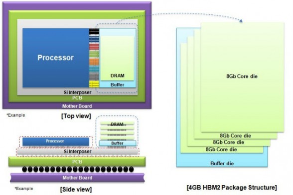
Samsung is able to realize this level of performance thanks to its TSV (Through Silicon Via) technology. By stacking HBM2 DRAM dies vertically, then connecting them through TSV technology, this provides significantly better data transmission performance compared to traditional wire-bonding technologies.
Currently Samsung is manufacturing their 4GB HBM2 packages with 8GB HBM2 packages coming by the end of the year. This should be very exciting with applications such as 4K and VR along becoming a lot more mainstream in 2016 and beyond.
Source: Samsung

