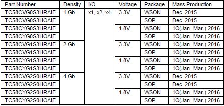
Toshiba recently introduced a new NAND family designed for embedded applications. The new NAND will be applied to consumer and industrial applications such as flat screen TVs, printers, wearables, and robots.
The new Toshiba NAND family offers a superior alternative to the NOR Memory typically used in embedded applications. SLC NAND memory is more cost effective, more reliable, and offer higher densities per package. These features are critical to store the increasingly complex software designed for today’s embedded devices.
The new NAND family can be controlled with just 6-pins, making it a suitable candidate for the Serial Peripheral Interface(SPI). The new NAND family can also be used as SLC NAND flash memory.
Specifications:
| Density | 1 Gb / 2 Gb / 4 Gb |
|---|---|
| Page Size | 2KB (1 Gb, 2 Gb), 4KB (4 Gb) |
| Interface | Serial Peripheral Interface Mode 0, 3 |
| I/O | x1, x2, x4 |
| Voltage | 2.7~3.6V, 1.7~1.95V |
| Operational Temperature Range | -40°C to 85°C |
| Package | 8pin WSON (6mm × 8mm), 16pin SOP (10.3mm × 7.5mm) |
| Features | High Speed Sequential Read, ECC, Data Protection, Parameter Page |
Toshiba has already begun shipping samples of this new NAND family. Full production for the 1 Gb module will begin in December 2015, with the rest to follow soon after.
Source: PR News Wire


