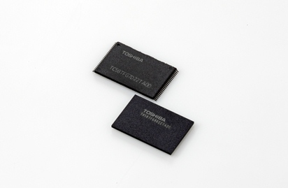
It’s been a little over half a year since Samsung launched their 3D NAND based Samsung 850 PRO, and it looks like Toshiba and SanDisk are finally making some inroads with their own 3D NAND technology as well.
According to recent press releases from both companies, Toshiba and SanDisk announced that they’ve completed development of the world’s first 48-layer 3D NAND product using their BiCS (Bit-Cost Scalable NAND) technology. As of now, very little information is known about the finalized BiCS product that’s being sampled however, we do know that BiCS will be based on charge trap technology rather than the older floating gate technology which is what Samsung uses in their 3D V-NAND.
The BiCS NAND now being sampled will be 2-bit MLC based with a maximum capacity of 128Gb (16GB) per die. I wouldn’t be surprised to see 3-bit MLC or higher die capacities when the dies begin shipping in retail products. Speaking of retail products, while samples are already shipping as of now, Toshiba and SanDisk don’t expect mass production to begin until at least 1H2016 when Fab2 at Yokkaichi Operations is completed. As such, products containing the new NAND shouldn’t be expected until 2H2016 at the earliest.
Currently, Samsung is the only company manufacturing products using 3D NAND. Both Intel/Micron and SK Hynix are expected to ship their first 3D NAND samples by mid-2015.
Update 03/26/2015: Intel/Micron recently held a webinar announcing that they’ve begun shipping 3D NAND as well.


